
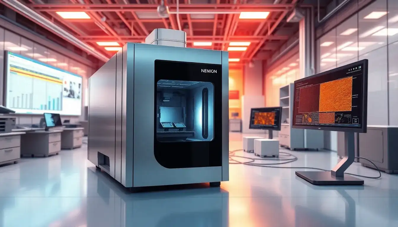
Applied Materials’ SEMVision™ G9: Pioneering a New Era of High-Throughput Defect Detection
During SEMICON China 2026, Applied Materials officially launched its next-generation platform, the SEMVision G9. This new product aims to enhance defect analysis capabilities, pushing advanced processes to new heights.
Recognized as the benchmark for defect detection, classification, and analysis, the SEMVision series has long supported global wafer fabs in improving yield and manufacturing efficiency. The SEMVision G9 is designed for defect detection applications in logic, memory, and other devices. It achieves scalable improvements in cross-platform defect detection and classification through more reliable imaging quality and integrated artificial intelligence (AI) technology, all while maintaining competitive total cost of ownership (CoO).
Why is the SEMVision G9 Important?
As device complexity continues to increase and 3D structures evolve, the distribution of defects has become denser, placing significant pressure on detection capabilities. The SEMVision G9 effectively expands detection capacity by supporting more detection sites and sample sizes at high speeds. This allows engineers to achieve full-layer coverage from front-end-of-line (FEOL) to back-end-of-line (BEOL) without sacrificing cycle time or overall ownership costs. Additionally, the integrated AI greatly reduces human involvement, shortens result acquisition times, and accelerates high-confidence production decisions.
Highlights of the SEMVision G9
- Enhanced Imaging Capability: Higher beam currents accelerate image acquisition speed. The improved maximum acceleration voltage, combined with the Elluminator™ wide-angle backscatter electron (BSE) detector, delivers superior image quality in challenging applications involving deeply buried defects and high aspect ratio structures.
- Exceptional Image Quality: The newly upgraded image processing algorithms effectively preserve defect signals under high noise conditions, providing industry-leading image quality.
- Upgraded Detection Speed and Process: Enhanced motion control and reduced repetitive processes during movement shorten end-to-end detection times.
- Proprietary AI Processes: The ADR AI, validated through large-scale production, supports single-image detection and CAD-based defect detection. Meanwhile, the ADC AI (Purity™ III) classification engine offers faster and more precise classification results.
- Continuity and Compatibility: The SEMVision G9 supports direct conversion and use of programs and imaging parameters from the industry-leading SEMVision G7, allowing performance improvements without interrupting production and providing a complete upgrade path from G7 to G9.
Key Applications of the SEMVision G9
As a leader in the defect detection field, the SEMVision G9 covers a wide range of application scenarios. It introduces several unique capabilities, including electron beam tilt, high-depth-of-field chamfer imaging, deep ultraviolet imaging suitable for bare chips and full wafers, material analysis, and the Elluminator wide-angle BSE detector.
In Summary
More wafers, deeper insights, and less manual intervention—SEMVision G9 combines trusted imaging technology with integrated AI to drive faster and more reliable production decisions.
Original article by NenPower, If reposted, please credit the source: https://nenpower.com/blog/semvision-g9-by-applied-materials-pioneering-a-new-era-in-high-capacity-defect-detection/