
1. The code for solar monocrystalline silicon A wafer incorporates specific classifications and identifiers associated with the manufacturing process, the physical characteristics, and the intended use of the material, emphasizing performance and quality. 2. This epitomizes a significant component in the photovoltaic industry, detailing various aspects such as efficiency ratings, dimensions, and purity standards that are essential for optimal energy conversion. 3. The codes utilized vary by manufacturer and application; however, they generally adhere to industry standards that provide a framework for evaluation. 4. Advances in wafer technology continue to evolve, highlighting the need for consistent coding to ensure compatibility across different systems and applications.
UNDERSTANDING MONOCRYSTALLINE SILICON A WAFERS
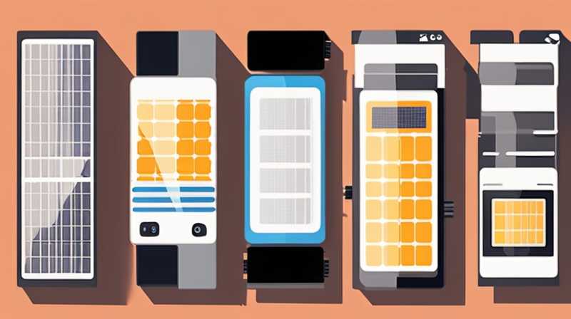
Monocrystalline silicon A wafers represent a crucial element in the solar energy sector. These wafers, characterized by their uniform crystal structure, contribute significantly to the efficiency and effectiveness of solar panels. The manufacturing process of these wafers involves a meticulous approach that ensures high levels of purity and structure, which directly correlates with their energy conversion capabilities. Recognizing the coding system associated with these wafers is essential for both manufacturers and consumers alike, as it guides the evaluation of their performance.
Manufacturing Process of Monocrystalline Silicon Wafers
The initial phase in creating monocrystalline silicon wafers involves deriving silicon from raw materials through processes such as carbothermic reduction. Following this step is the crystallization process, which can utilize methods like the Czochralski process or the float zone method. In the Czochralski technique, a seed crystal is dipped into molten silicon, and as it is slowly withdrawn, it forms a larger crystal structure. This structure is then sliced into wafers of varying thicknesses depending on the specific application requirements. Each of these wafers is scrutinized to ensure it meets stringent purity and structural integrity standards, making this phase critical in achieving the desired performance outcomes.
Furthermore, elements such as doping are introduced during the manufacturing phase to enhance electrical conductivity. The incorporation of materials like phosphorus or boron creates p-type or n-type silicon, respectively, which significantly affects the electrical characteristics of the wafers. Consequently, the codes associated with solar monocrystalline silicon A wafers often indicate the type of doping, purity levels, and other properties fundamental for solar cell applications.
Performance and Efficiency Metrics
Performance metrics linked with monocrystalline silicon A wafers are predominantly defined by their efficiency rates, which can vary based on manufacturing practices and the purity of the silicon used. These efficiency ratings are vital for consumers and industries since they directly impact the energy output and overall effectiveness of solar panels. The standard for efficiency in monocrystalline silicon is often benchmarked against the theoretical maximum efficiency of around 26.7% for silicon-based cells.
Moreover, the size and thickness of the wafers play a critical role in their performance. Thinner wafers, while reducing material costs, have to balance durability, functionality, and efficiency. Manufacturers often resort to optimizing thickness to ensure that the wafers can withstand various stressors while maintaining a high degree of performance. Accordingly, the associated codes will include specific numerical values that correspond to these dimensions.
INDUSTRY STANDARDS & CLASSIFICATIONS
The solar industry operates under various standardization organizations that provide guidelines and classifications for monocrystalline silicon A wafers. These standards play an essential role in ensuring that products are manufactured to the expected specifications globally. Notable organizations like the International Electrotechnical Commission (IEC) and the Underwriters Laboratories (UL) supply the directives that govern the manufacturing processes and quality assurance testing of solar panels.
Importance of Certification Standards
Certification standards enhance consumer confidence by guaranteeing that the products meet international safety and performance criteria. Products certified by these bodies are typically subjected to comprehensive testing for efficiency, insulation resistance, and overall durability to environmental factors. For instance, IEC 61215 is a critical standard that evaluates the design and performance of solar modules under various stress conditions, ensuring long-term reliability.
Moreover, having a consistent coding system aids manufacturers in compliance with local regulations and international trade agreements. This uniformity streamlines communication between manufacturers and suppliers, facilitating smoother transactions and enhancing transparency throughout the supply chain. Consequently, adherence to these standards and certifications is crucial for market growth and the advancement of solar technology.
Diversity in Coding Systems Across Manufacturers
While industry standards provide a framework, different manufacturers may employ their unique coding systems that represent their specific processes and attributes. This variation can lead to confusion in the marketplace, where the same type of wafer may carry different codes depending on the producer. Properly understanding these codes is integral for stakeholders in the solar industry, including project developers, installation companies, and end-users.
For instance, the code may incorporate information about the batch number, material specifications, efficiency rating, and manufacturing location. By deciphering these codes, professionals in the industry can make informed decisions regarding procurement, installation, and system design, ultimately influencing the project’s success.
ADVANCEMENTS IN TECHNOLOGY
The continuous evolution in technology has led to the development of innovative manufacturing processes and materials, enhancing the performance of monocrystalline silicon wafers. Recent advancements focus on increasing the energy conversion rates while minimizing production costs, ensuring that solar energy remains a viable alternative to fossil fuels.
Emergence of High-Efficiency Wafer Technologies
One noteworthy development in this arena is the creation of high-efficiency bifacial solar cells. These cells capture sunlight on both sides, harnessing reflected light from surfaces underneath the installation. The coding for these wafers often includes identifiable markers denoting bifacial capabilities, offering insights into their enhanced performance metrics compared to traditional cells.
Another breakthrough involves the adoption of passivated emitter and rear cell (PERC) technology. PERC cells utilize an additional layer on the rear side of the wafer to minimize energy loss, thereby improving the overall efficiency. Coding systems for these advanced technologies will typically highlight the incorporation of such features, helping stakeholders evaluate their options based on performance benefits.
Sustainability in Manufacturing Processes
Sustainability has emerged as a critical principle in the solar industry, with efforts directed toward reducing the environmental impact of wafer production. Innovations in recycling silicon waste from the manufacturing process contribute to creating more sustainable operations, while also providing cost-saving opportunities for manufacturers. Coding systems for environmentally friendly wafers may carry indicators or labels denoting their sustainable origins, acting as a selling point for eco-conscious consumers.
Through the lens of sustainability, the solar energy sector is witnessing a shift towards a more responsible manufacturing approach, aligning with global calls for greener technologies and practices. Thus, the coding of solar monocrystalline silicon A wafers is evolving to encapsulate these values, presenting an opportunity for businesses to demonstrate their commitment to sustainability.
FUTURE TRENDS IN SOLAR TECHNOLOGY
As the exigencies of the climate crisis intensify, the solar industry is projected to advance at an accelerated pace, with monocrystalline silicon A wafers playing a fundamental role in this transition. Upcoming trends suggest a shift towards integration with innovative technologies, optimization of existing resources, and improvements in efficiency.
Integrating Renewable Energy with Smart Technologies
The future of solar technology lies in its integration with smart energy solutions, including energy management systems and grid interconnectivity. Monocrystalline silicon A wafers will be instrumental in facilitating this transition by serving as reliable energy sources that can be synchronized with smart grids. This blend of technologies is anticipated to enhance energy storage capabilities and promote effective distribution across urban and rural landscapes.
In addition, coding for future solar wafers may embody data-driven insights that contribute to real-time performance tracking and optimized energy output. Such innovations may allow for proactive maintenance strategies, effectively reducing downtime and increasing energy generation over the lifecycle of photovoltaic systems.
Exploring Perovskite-Silicon Hybrids
The exploration of hybrid solar cells reflecting the amalgamation of perovskite and silicon technologies signifies a noteworthy trend. These hybrid structures offer the potential for even higher energy conversion efficiencies compared to traditional monocrystalline cells. As research continues to unravel the practical aspects of these materials, it is plausible that the coding systems will accommodate both the silicon attributes and the unique properties of perovskite materials, signaling a new era in solar technology.
In conclusion, the innovation trail in the solar energy industry remains vibrant as stakeholders engage in addressing urgent global energy needs through advanced materials and technologies. Monocrystalline silicon A wafers are at the forefront of this revolution, anchoring a sustainable and efficient energy future.
COMMON QUERIES ABOUT MONOCRYSTALLINE SILICON A WAFERS
WHAT ARE MONOCRYSTALLINE SILICON WAFERS USED FOR?
Monocrystalline silicon wafers are primarily used in the manufacturing of solar cells for photovoltaic systems. Their uniform crystal structure allows for higher energy conversion efficiencies compared to polycrystalline alternatives. This characteristic makes them a highly sought-after component in solar panel production, especially for applications requiring robust power generation in diverse environmental conditions. Furthermore, due to their higher efficiency ratings, these wafers can generate more energy from a given area of sunlight, which is essential in maximizing energy output in limited spaces.
Additionally, monocrystalline silicon wafers are integral in specialized applications such as satellites, where weight and efficiency are vital. The lightweight properties and efficiency of these wafers facilitate their implementation in aerospace technologies. Due to their extensive applicability across various sectors, monocrystalline silicon wafers are poised to play a significant role in the ongoing transition towards renewable energy.
HOW DO MANUFACTURING PROCESSES AFFECT WAFER PERFORMANCE?
The manufacturing processes directly influence the performance, quality, and efficiency of monocrystalline silicon wafers. Key factors such as raw material purity, crystal growth methodology, and doping techniques contribute to the final product’s capabilities. For instance, the choice between the Czochralski and float zone methods can result in variances in crystal quality and defect density, which subsequently impact electrical characteristics.
Moreover, the treatment processes that wafers undergo post-manufacturing, such as passivation and texturing, are equally critical. Effective surface treatment can minimize recombination losses, maximizing the wafers’ ability to convert sunlight into energy. Therefore, the sophistication of manufacturing techniques and adherence to standards significantly dictate the overall performance potential of monocrystalline silicon wafers.
WHAT ARE THE ADVANTAGES OF MONOCRYSTALLINE SILICON OVER POLYCRYSTALLINE SILICON?
Monocrystalline silicon holds several distinct advantages when compared to polycrystalline silicon, primarily concerning efficiency and space utilization. The uniform crystal lattice of monocrystalline silicon wafers enables them to achieve higher efficiency ratings, translating to greater electricity generation per square meter of panel. This efficiency is particularly beneficial in scenarios where space is limited, such as urban environments or on rooftops.
Furthermore, monocrystalline silicon panels typically have better performance in low-light conditions, enhancing energy yield during cloudy days or in shaded environments. Durability is another asset, as these wafers often have longer operational lifespans, resulting in decreased costs over the lifecycle of installations. Thus, for many consumers and businesses, the superior aspects of monocrystalline silicon solidify its position as the preferred choice in the solar market.
THE SIGNIFICANCE OF SOLAR MONOCRYSTALLINE SILICON A WAFER CODES
The coding system associated with monocrystalline silicon A wafers serves as a critical tool for ensuring product quality, performance traits, and compatibility with various applications in the solar energy landscape. Through precise classification, it fosters an understanding among manufacturers and consumers regarding the various specifications, efficiencies, and intended uses of the products. The integration of advanced manufacturing techniques, coupled with the establishment of rigorous standards, further emphasizes the importance of these codes in supporting the evolving demand for high-efficiency solar energy solutions.
As solar technology advances toward a more sustainable future, the significance of accurate coding will only escalate. It will become vital to uphold transparency in manufacturing practices while ensuring that products adhere to established safety and performance benchmarks that benefit end-users dramatically. Correspondingly, stakeholders will need to cultivate a solid understanding of these coding systems to make informed decisions that not only contribute to energy sustainability but also to the broader effort of combating climate change. The trajectory of solar monocrystalline silicon A wafers will reflect the industry’s commitment to innovation, efficiency, and environmental stewardship.
Original article by NenPower, If reposted, please credit the source: https://nenpower.com/blog/what-is-the-code-for-solar-monocrystalline-silicon-a-wafer/
