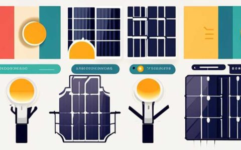
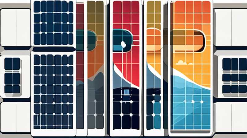
Solar photovoltaics (PV) primarily utilize silicon-based chips, thin-film technologies, and multi-junction solar cells. 1. Silicon-based chips dominate the market due to their high efficiency and cost-effectiveness. 2. Thin-film technologies employ materials such as cadmium telluride and amorphous silicon, providing flexibility and lightweight options. 3. Multi-junction solar cells utilize multiple semiconductor layers to capture different wavelengths of light, enhancing overall energy conversion efficiency. 4. Emerging technologies like perovskite and organic photovoltaic cells are also gaining traction, offering potential for lower production costs and versatile applications. Among these innovations, silicon-based chips stand out as the most widely used and commercially viable for current solar energy systems, primarily due to their established manufacturing processes and lifetime performance.
1. SILICON-BASED CHIPS
Silicon has held the crown in the realm of solar photovoltaic technology for decades, serving as the backbone for a majority of solar panels installed globally. The roots of this dominance are intertwined with various unique attributes that silicon offers, making it exceptionally suitable for harnessing solar energy. Historically, silicon-based PV cells were among the first to achieve commercial viability, largely due to their ability to efficiently convert sunlight into electricity.
In silicon’s crystalline form, the chips are categorized into single-crystalline and polycrystalline types. Single-crystalline silicon chips are known for their high efficiency rates, often exceeding 20%. They are manufactured from high-purity silicon, resulting in a uniform structure that facilitates better electron flow. In contrast, polycrystalline silicon chips, while slightly less efficient, offer a more environmentally friendly and less expensive production method. Their manufacturing process involves melting raw silicon and pouring it into molds, which is much more resource-efficient than the method used for single-crystalline silicon. Additionally, the scaling of production for polycrystalline wafers has led to a reduction in costs, making them attractive for large-scale solar installations.
The efficiency and longevity of silicon-based technologies make them the preferred choice in a variety of applications, from residential rooftops to large solar farms. While other materials may offer innovative benefits, the resilience of silicon technology, including its response to environmental factors, continues to make it a mainstay in photovoltaic use. Research into improving the efficiency of silicon solar cells is ongoing, with aspirations to push the boundaries beyond 25%, thus solidifying its position in future solar innovations.
2. THIN-FILM TECHNOLOGIES
Advancements in solar technology have paved the way for thin-film technologies, which have carved out their niche in the competitive solar market. Combining lightweight and flexible attributes with a less resource-intensive manufacturing process, thin-film solar panels present an appealing alternative to traditional silicon chips. Notably, materials such as cadmium telluride (CdTe), copper indium gallium selenide (CIGS), and amorphous silicon are often utilized in thin-film applications, each with distinct advantages and challenges.
Cadmium telluride is one of the most widely deployed thin-film technologies, primarily due to its favorable cost-to-efficiency ratio. CdTe modules can achieve efficiencies around 11-12%, which while lower than the traditional silicon solar cells, can still be competitive when factoring in the reduced production costs. This technology is particularly beneficial for utility-scale solar farms, where the lower weight and flexibility allow for rapid deployment on a wider range of surfaces without structural reinforcement.
Similarly, copper indium gallium selenide has gained traction for its unique characteristics. CIGS solar cells are recognized for their high absorption coefficient and potentially greater efficiency compared to other thin-film technologies. Laboratory tests have shown efficiencies exceeding 22%. However, the complex manufacturing process for CIGS can lead to higher costs, limiting its market penetration compared to CdTe.
Furthermore, the lightweight nature of thin-film technologies enables their integration into various surfaces, including building-integrated photovoltaics (BIPV) that merge seamlessly into architectural designs. The innovation potential in the thin-film domain shows promise, especially as developers and researchers explore new materials to enhance efficiency, durability, and production when compared to traditional silicon solutions.
3. MULTI-JUNCTION SOLAR CELLS
Innovations in photovoltaic technology continue to push the boundaries of efficiency and performance, leading to the development of multi-junction solar cells. By stacking multiple layers of semiconductor materials, each optimized for capturing different segments of the solar spectrum, these advanced cells maximize light absorption and energy conversion. The multi-junction approach is primarily utilized in specialized applications such as space exploration and concentrated solar power systems, where high efficiency is paramount.
The most notable feature of multi-junction solar cells is their layered architecture, which typically incorporates combinations of materials such as gallium arsenide (GaAs) and indium phosphide (InP). Each layer is designed to absorb specific wavelengths of sunlight, capturing a broader range of the solar spectrum compared to single-layer technologies. This capability allows them to achieve astonishing efficiency rates, often exceeding 40% in lab settings. However, the production costs of multi-junction solar cells remain prohibitively high compared to conventional silicon-based systems, making their widespread adoption a challenge.
Moreover, multi-junction technology excels in environments where space is limited but power output must be maximized, such as on rooftops in urban areas or in satellite applications. Their lightweight and high-performance characteristics make them suitable for a variety of cutting-edge applications. As research progresses, efforts to reduce production costs while maintaining performance have the potential to revolutionize their use in the commercial sector.
As these technologies evolve, the integration of multi-junction systems into broader energy strategies holds promise for harnessing a greater amount of solar energy. While challenges remain, the pursuit of efficiency in solar energy harvesting continues to inspire significant advancements in this area.
4. EMERGING TECHNOLOGIES
With an ever-evolving landscape, emerging technologies in solar photovoltaic systems are on the cusp of changing the dynamics of energy generation. Developments such as perovskite solar cells and organic photovoltaics (OPVs) are gaining attention due to their unique properties and potential for cost-effective production. These technologies could disrupt conventional silicon and thin-film markets by offering innovative approaches to energy conversion.
Perovskite solar cells represent a new frontier marked by their simple manufacturing process and impressive efficiency. Made from a class of materials that can easily be processed from solution, perovskite cells can reportedly reach efficiencies of over 25% in laboratory settings. This remarkably low-cost fabrication process makes it feasible to produce solar panels on flexible substrates, opening doors for applications that were previously unachievable. However, stability and long-term performance remain concerns that researchers are actively addressing.
Organic photovoltaics, using carbon-based materials for solar energy conversion, also show significant promise. OPVs can be produced through low-cost printing techniques, allowing for rapid scaling and a diversity of designs that can be integrated aesthetically into buildings and products. While the efficiency of OPVs is currently lower than traditional methods, ranging between 10-15%, ongoing research aims to improve performance while maintaining the advantages of flexibility and lightweight characteristics.
Both perovskites and organic materials contribute to a critical vision of the solar energy future, focused on sustainability, adaptability, and economic viability. By broadening the solar market and enabling diverse applications, these emerging technologies may very well redefine the role of photovoltaics in global energy strategies.
FREQUENTLY ASKED QUESTIONS
WHAT ARE SILICON-BASED SOLAR CHIPS?
Silicon-based solar chips predominantly serve as the foundational technology in the photovoltaic sector, recognized for their robustness and efficiency. These chips primarily encompass two types: monocrystalline and polycrystalline. Monocrystalline silicon is valued for its single-crystal structure which allows for higher efficiency rates, typically exceeding 20%. This structure minimizes defects that can hinder performance, enabling superior electron movement.
On the other hand, polycrystalline silicon offers a cost-effective alternative. The production method involves melting raw silicon and cooling it in bulk, leading to a less organized crystal arrangement, which results in slightly lower efficiency. However, the significant reduction in manufacturing costs positions polycrystalline silicon favorably in large-scale solar installations. The choice between these types often hinges on balancing efficiency and cost, making silicon-based chips a mainstay in solar technology. Ongoing research continues to enhance the efficiency and durability of these solar cells, affirming their relevance as industries evolve.
HOW DO THIN-FILM SOLAR CELLS COMPARE TO TRADITIONAL SILICON CELLS?
Thin-film solar cells offer a different approach to solar energy conversion when compared to traditional silicon cells. While traditional silicon cells are characterized by their crystalline structure—either mono or polycrystalline—thin-film solar cells utilize a layer of semiconductor material deposited on a substrate. This method provides several advantages, primarily flexibility and lightweight characteristics, making thin-film panels easier to install in varied applications, including building-integrated photovoltaics.
Despite their advantages, thin-film cells generally have lower efficiency rates, approximately 10-12% for cadmium telluride cells and around 11-14% for copper indium gallium selenide. In contrast, silicon-based cells can achieve efficiencies of 15-22%. However, the reduced material requirements can lead to lower manufacturing costs, offering thin-film technology as a viable alternative, especially for large-scale utility projects where the cost per watt is critical. The decision between the two technologies largely depends on the specific application, budget constraints, and performance expectations, highlighting the continued relevance of both approaches in diverse environments.
WHAT ARE MULTI-JUNCTION SOLAR CELLS AND THEIR ADVANTAGES?
Multi-junction solar cells represent an innovative advancement in photovoltaic technology, effectively stacking multiple layers of semiconductor materials to optimize sunlight absorption. Each layer is tailored to capture different wavelengths of light, significantly enhancing overall energy conversion efficiency compared to single-junction technologies. This design allows multi-junction cells to achieve impressive efficiency rates, often surpassing 40% in laboratory conditions.
The utility of multi-junction solar cells extends into specialized applications, particularly where space is limited but high power output is essential, such as in space missions and high-efficiency concentrated solar power systems. However, the manufacturing costs remain high, which can limit their applicability in mainstream residential or commercial contexts. Research initiatives aim to streamline production processes and cost structures to make multi-junction technologies commercially viable. As this technology matures, its contribution to efficient renewable energy production holds significant potential for the future.
Advancements in solar photovoltaic technologies have burgeoned in recent years, reflecting a dynamic interplay of materials innovation and engineering efficiency. The continual presence of silicon-based chips in the solar market speaks volumes about their established production and overall viability. Meanwhile, thin-film technologies have carved out an influential niche by providing flexibility, albeit typically with reduced efficiency. The emergence of multi-junction solar cells further demonstrates the industry’s commitment to maximizing energy conversion by leveraging layered semiconductor technologies, although high costs pose significant barriers to widespread adoption. Lastly, the prospective rise of novel materials, particularly perovskite and organic photovoltaics, offers a glimpse into a future where solar energy becomes even more accessible and economically feasible. Each of these advancements encapsulates broader trends in sustainable energy, illustrating the inexorable march toward more efficient, diversified, and integrated solar energy solutions in contemporary society. As the landscape of solar energy continues to evolve, the collective insights gleaned from these technologies usher us into an era of innovation that holds promise for overcoming both ecological and economic challenges through renewable resources.
Original article by NenPower, If reposted, please credit the source: https://nenpower.com/blog/what-chips-are-used-in-solar-photovoltaics/