
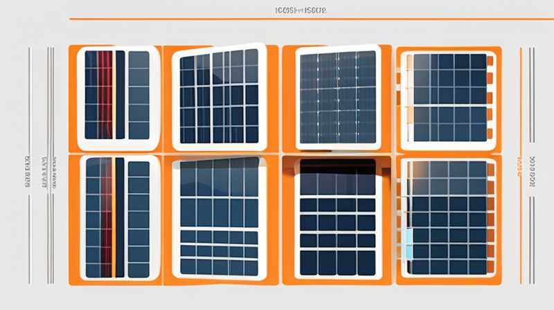
To produce solar photovoltaic panels, multiple steps are involved, encompassing material selection, processing techniques, and assembly methods. 1. The initial step requires the choice of semiconductor materials, such as silicon, which are crucial for energy conversion. 2. Subsequently, these materials undergo intensive purification and crystallization processes to ensure efficiency. 3. After preparation, the materials are sliced into thin wafers that serve as the foundation for the panels. 4. Once the wafers are ready, they are treated with various doping agents to enhance their electrical properties. 5. Finally, the assembled units undergo rigorous testing to ensure functionality and longevity. Each of these steps plays a pivotal role in the final output, reflecting the complexity and advanced technology involved in solar energy harvesting.
1. UNDERSTANDING SOLAR PHOTOVOLTAIC TECHNOLOGY
The advancement of solar photovoltaic technology is a cornerstone in the realm of renewable energy. This specific technology allows for the direct conversion of sunlight into electricity through the photovoltaic effect. The significance of this form of energy cannot be overstated as it aligns seamlessly with global initiatives aimed at reducing reliance on fossil fuels and mitigating climate change.
When examining solar photovoltaic panels, one recognizes that they consist of interconnected solar cells, typically made from silicon-based materials. This strategy not only maximizes energy capture but also enhances the panel’s overall efficiency. An understanding of the underlying science, including how photons interact with semiconductors, provides insight into the potential these panels hold for energy production on a significant scale.
Moreover, technological advancements have led to the exploration of alternative materials and designs, such as thin-film technology and multi-junction cells. Each innovation aims to improve efficiency rates, decrease production costs, and increase versatility in deployment. As global energy demands rise, innovative solutions within solar photovoltaic technology will be crucial for sustainable development.
2. MATERIAL SELECTION AND PURIFICATION
The selection of materials serves as the foundation of manufacturing solar photovoltaic panels. Silicon remains the predominant choice due to its optimal semiconductor properties and abundance. However, the purity of silicon directly influences the panel’s efficiency; thus, the purification process involved is critical.
Silicon extraction begins with the mining of quartz, which is then refined to extract metallurgical-grade silicon. This initial step leads to the production of silicon of varying purity levels. For solar applications, silicon must reach a purity level of 99.9999% (6N). This demanding requirement is achieved through processes such as the Siemens process and the Czochralski process. The latter involves melting silicon crystals within a controlled environment, leading to a single crystal structure that optimizes energy conversion.
Beyond silicon, research has also gravitated towards alternative materials, such as cadmium telluride and gallium arsenide. While these materials offer unique advantages, they come with specific manufacturing challenges and considerations that can impact large-scale implementation. Thus, selecting the most appropriate material is a multifaceted decision, weighing both costs and performance metrics.
3. WAFER PRODUCTION AND DOPING PROCESSES
Upon successful material purification, the next stage involves the production of wafers. Wafer fabrication is pivotal, transforming the bulk material into thin slices that serve as the backbone of solar cells. The thickness of these wafers dramatically affects both the cost and the efficiency of the final product.
Using advanced slicing technologies, silicon is cut into wafers typically ranging from 180 to 220 micrometers in thickness. This precision is necessary not only to minimize waste but also to ensure optimal performance in energy conversion. Post-slicing, the wafers undergo various processes such as etching and surface texturing to enhance their light-absorbing capabilities.
Doping is another critical aspect, wherein specific impurities are introduced to alter the electrical properties of the silicon. Through processes like phosphorus and boron doping, the wafers can be engineered to create p-n junctions—essential for forming the electric field necessary for current generation. The careful management of doping concentrations directly correlates to the efficiency of the final solar cell.
4. ASSEMBLY OF PHOTOVOLTAIC PANELS
The assembly stage brings together individual solar cells to form a cohesive panel. This intricate process begins with the selection of appropriate encapsulation materials that protect the cells from environmental factors such as moisture and temperature fluctuations. Typically, ethylene-vinyl acetate (EVA) is used as an encapsulant due to its excellent adhesive properties and transparency.
In addition to protection, the arrangement of cells within the module needs to be optimized for energy output. Cells are interconnected using conductive ribbons, ensuring efficient electricity flow. As the final assembly takes place, the panel is framed and fitted with protective glass, serving as both a shield against the elements and a mechanism to prevent damage.
Further considerations must also include the junction box installation, allowing for electrical connections and system integration. The synergy of all these components culminates in a fully functional solar photovoltaic panel capable of converting sunlight into usable power. This part of the process exemplifies how engineering, design, and advanced materials science interconnect within solar technology.
5. TESTING AND QUALITY ASSURANCE
Quality assurance is paramount in the solar panel manufacturing process. Each unit undergoes a series of tests designed to ensure reliability, efficiency, and robustness before reaching the market. Testing methodologies include visual inspections, electroluminescence testing, and performance audits under various environmental conditions.
Electroluminescence testing serves as a vital tool, identifying potential defects within solar cells that may not be visible by the naked eye. By passing a current through the cells and observing light emissions, manufacturers can detect issues related to cell integrity. This non-destructive method ensures that only panels meeting stringent quality standards are deployed.
Environmental testing further assesses durability; panels are subjected to extreme conditions such as high temperatures, humidity, and mechanical stress. Such rigorous evaluations help ascertain that the panels can withstand the operational demands over an extended lifespan, ensuring consistent performance for consumers.
6. FUTURE TRENDS IN SOLAR PHOTOVOLTAIC MANUFACTURING
As the demand for solar energy continues to escalate, future trends in solar photovoltaic manufacturing are pivotal for driving efficiency and scalability. Innovations such as bifacial panels are gaining traction owing to their ability to capture sunlight from both sides, significantly enhancing energy generation.
Additionally, the integration of artificial intelligence in manufacturing processes allows for smarter, adaptive production techniques. These technologies enable real-time monitoring of manufacturing conditions and booth performance, leading to reduced waste and improved yield.
Research into perovskite solar cells has also shown considerable promise, with the potential to disrupt traditional silicon-based technology. These cells offer the advantages of lower production costs and enhanced efficiency, positioning them as a competitive alternative in the marketplace. Continuous advancements in materials science and engineering practices will likely shape the future landscape of solar photovoltaics, ensuring sustainable energy solutions for generations to come.
QUESTIONS AND RESPONSES
WHAT MATERIALS ARE USED IN SOLAR PHOTOVOLTAIC PANELS?
The most prevalent materials in solar photovoltaic panels are silicon-based, particularly crystalline silicon and thin-film technologies. Crystalline silicon is known for its superior efficiency and performance, while thin-film materials, like cadmium telluride and copper indium gallium selenide, offer flexibility in production. Each material has unique properties that impact the panel’s efficiency, cost-effectiveness, and energy output.
Crystalline silicon panels can be further classified into monocrystalline and polycrystalline types. Monocrystalline panels, made from single crystals, tend to be more efficient and space-efficient, making them ideal for residential applications with limited rooftop space. Polycrystalline panels, created from multiple silicon crystals, are generally less expensive but may offer lower efficiency levels.
On the other hand, thin-film technologies are easier and cheaper to manufacture. They can be flexible and lightweight but often do not match the efficiency levels of crystalline counterparts. The choice of material must align with specific energy requirements, budgetary constraints, and intended use cases.
HOW ARE SOLAR PANELS TESTED FOR QUALITY?
Quality testing protocols for solar panels ensure that each unit meets safety and performance standards necessary for consumer use. The testing process begins with visual inspections to identify any physical defects or build quality issues. Panels are then subjected to rigorous performance assessments, simulating real-world conditions they will face.
One of the primary methods employed is electroluminescence testing, which detects defects in the solar cell structure via an electric current that causes cell illumination. This testing highlights potential issues, such as micro-cracks or broken cells, which could impact efficiency.
Furthermore, climate exposure tests simulate extreme weather conditions, including hail trials, high-heat environments, and moisture resistance. These assessments ascertain that the solar panels can endure a variety of stresses encountered over their operational lifespan. A combination of these methodologies ensures that only quality assured solar panels reach the market, thus providing reliability for consumers.
WHAT IS THE AVERAGE LIFESPAN OF SOLAR PANELS?
On average, solar photovoltaic panels have a lifespan of approximately 25 to 30 years, although many can operate efficiently well beyond this period. Several factors contribute to this longevity, including the quality of materials used, manufacturing practices, and environmental conditions where the panels are installed.
Most manufacturers offer warranties that guarantee a minimum performance level for 25 years, ensuring that panels will produce a certain percentage of their rated power output during that time. It’s essential to maintain the panels, cleaning them regularly and ensuring they are free from debris or shading that could reduce efficiency and lifespan.
Moreover, advancements in technology are starting to extend the longevity of solar panels. Innovations in encapsulation materials and enhanced protective layers are driving improvements in durability and efficiency. As these technologies develop, the expectation is that future-generation solar panels will not only last longer but also maintain higher efficiency levels throughout their life cycles.
Ultimately, the production of solar photovoltaic panels entails a sophisticated interplay of science, engineering, and innovation. Drawing on diverse materials and advanced techniques, the industry seeks to foster sustainable energy solutions. Moreover, continuous research and advancements will be critical as public and governmental demand for renewable energy rises. By understanding the intricacies of solar panel manufacturing, consumers, and industries can better appreciate the role of solar energy in a sustainable future.
Original article by NenPower, If reposted, please credit the source: https://nenpower.com/blog/how-to-make-solar-photovoltaic-panels-2/
